
Ensuring signal integrity has never been more critical than in a world dominated by data rates that just keep climbing. As signals travel at such high speeds and frequencies, the intricacies of radio frequency PCB layout optimization have become critical hardware solution, to say the least. This ultimate guide will delve into this deeply affecting aspect of PCB design for high-speed and high-frequency applications such as wireless communication and cutting-edge radar systems. You won’t want to miss it, as this guide allows you to figure out the RF PCB layout best practices and take your signal integrity skills to the next level.
1. Understanding Signal Integrity in RF Designs
Understanding the importance of signal integrity is crucial for RF designs. The concept revolves around whether the signal maintains its sharp shape and properties as it meanders through the twisted maze of components and interlinks on a PCB. In the high-stakes environment of RF applications, signal integrity is more than just essential; it is an absolute necessity. A small amount of distortion or interference can spread to the rest of the system and seriously compromise its performance. When you learn the intricacies of signal integrity, you essentially discover the secret to maximizing the potential of your RF designs—guaranteeing that they function with pinpoint accuracy and dependability.
2. The Importance of Proper RF PCB Layout
In the intricate dance of RF design, the PCB layout serves as the conductor, directing the invisible orchestra of signals. An improperly constructed layout would render a signal reflection a disruptive echo, crosstalk an unequaled disturbance, and EMI an unrelenting hum. As you have already gathered, this veritable symphony of issues would have a damning impact on the overall performance; a poor layout inevitably influences signal quality, reduces transmission range, and allocates the risk of failing the whole system. Yet, with meticulous optimization, the layout transfigures the aforementioned cacophony of disasters into a virtuoso-like peak of performance. Thus, across the precarious realm of RF design, the adeptly fitted layout is the maestro, enabling every component and harmonizing your design.
3. Impedance Matching and Controlled Impedance
Impedance matching is a fundamental concept to be in the realm of RF PCB design – a principle that cannot be neglected. If disregarded, impedance mismatches can set off a chain reaction of signal reflections, sent back down the circuit like deranged voices in a canyon – soon, standing waves will develop and destroy your signal, dissipating precious power. The only way to prevent such a mess is to employ controlled impedance measurements. However, much like the conductor of an orchestra, these measurements must be timed, calculated, and maintained throughout the signal path with expert precision. Only then can the symphony of your RF design truly sing – free of impedance mismatching.
4. Trace Routing and Length Matching
The pathway these delicate and sensitive signaling filaments take throughout an RF PCB is quite crucial in all of this. The conductive paths between devices must be direct and brief. A signal down a filaments path’s journey can be slowed by echoes or inadvertently triggered detours, disrupting the symphony. But it becomes different when complex designs enter the realm of possibility and normalcy. Signal-steps must step in time comparable to the An adjacent I2C channel that crops up here, not quite as severe but to consider. SDF delivers the ultimate ability of symmetry to coordinate developments, and to implement such miracles, signal paths within RF PCBs embrace equivalent pursuit. Thus, utilizing precisely guided traces contrast in total span allows designers to master tremendous symphonies of circuit paths where every flute, every beat sounds in harmony.
5. Ground Plane and Power Plane Considerations
Both good grounding through power distribution network (PDN) and power distribution network (PDN) are vital for signal integrity on RF printed circuit boards (PCBs) for the hardware designer. A solid one earth ground plane which is also uninterrupted is an effective EMI suppressor and it provides a low-impedance return path for the signals. Furthermore, a properly designed power plane guarantees this in turn and proves to be the right way of power delivery for the hardware designer. The voltage shortages and noises are avoided as expected.
6. Component Placement and Layout
Component placement on the PCB has a lot of influence on signal integrity; RF components such as amplifiers, filters, and antennas should be well arranged to minimize coupling and interference. Moreover, highly sensitive RF traces should be placed away from high-speed digital signals and power planes to avert crosstalk and avoid noise coupling.
7. Shielding and Isolation Techniques
The world of RF designs is cacophonic, with electromagnetic interference and signal coupling poised to break up the tender symphony. But some techniques serve as measures of shielding and isolation — the guardians of RF. Using grounded guard rings and cautiously positioned partitions or cavities and assembling shielding cans resembles constructing an impregnable fortress – a sanctuary that isolates and safeguards delicate RF components and routes . Here, the noisy whispers of external disturbance and inner noise sources perish away, and your design’s flawless overtones resound chaste, keeping each harmonic signal’s purity.
8. Simulation and Verification
Prior to the manufacture of an RF PCB, it is necessary to conduct simulation and verification exercises to spot the attendant signal integrity failures. Tools of electromagnetic simulation can model signal behavior, impedance, and crosstalk effects, providing designers with a chance to fix the situation and improve the production preliminarily.
9. PCB Material Selection
One of the most important factors affecting signal integrity in high-frequency RF applications is the PCB material chosen. The ideal material should exhibit low dielectric loss and have a stable and very low dielectric constant, ensuring minimal signal attenuation and uniform impedance. Moreover, the material should have excellent dimensional stability and low moisture absorption, allowing it to perform reliably in a variety of environmental conditions.
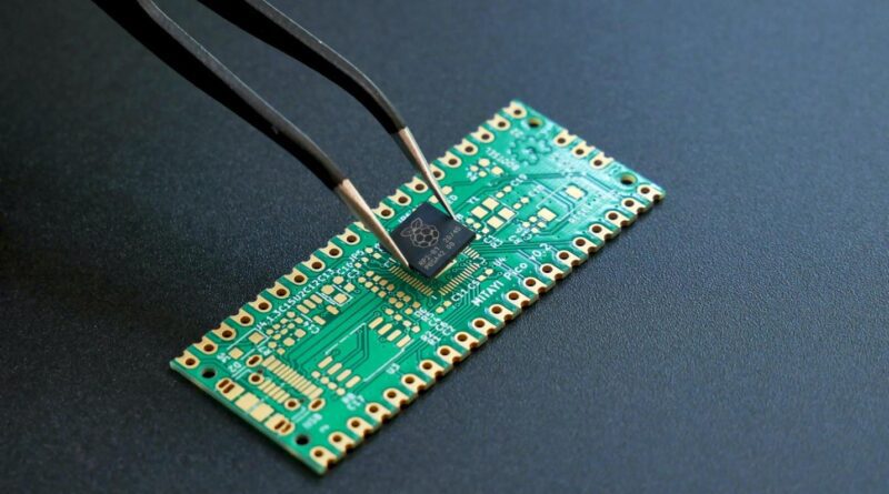
10. Manufacturing and Assembly Considerations
The quality of PCB material chosen could have a major influence on signal integrity, notably regarding RF applications with high frequency. Materials with less dielectric loss and consistent dielectric constant are preferred to lessen signal attenuation and maintain consistent impedance. Materials with reduced moisture absorption and thermal performance are also desirable to guarantee adequate performance in different environmental circumstances.
Conclusion
Signal integrity optimization in RF PCB layouts for vlsi system on chip design is a complex and multifaceted task. Designers can master it and ensure signal self-respect, serving this guide on the highest principles. Impedance matching and using controlled impedance, proper grounding and component placement, good shielding – everything should be treated with the same attention since each of these aspects plays a significant role in the overall result.